IC TRNSLTR BIDIRECTIONAL US8
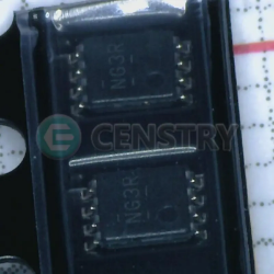
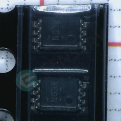


图片仅供参考.
有关产品详细信息,请参阅产品规格。
IC TRNSLTR BIDIRECTIONAL US8
订单满$200即可获赠限量版中式礼品一份.
订单金额超过 1000 美元可减免 30 美元运费.
超过 5000 美元的订单可免运费和交易费.
这些优惠适用于新客户和现有客户,有效期为2024年1月1日至2024年12月31日.
TI
TXS0102QDCURQ1 datasheet
VSSOP8
IC芯片
 Lead free/RoHS Compliant
现在提交您的报价请求,我们期望在 六月 30, 2024内提供报价。现在就下订单,我们期望在 七月 04, 2024内完成交易。时间是格林威治标准时间+8:00。


1 Features
• Qualified for Automotive Applications
• AEC-Q100 Qualified With the Following Results:
– Device Temperature Grade 1: –40°C to 125°C Ambient Operating Temperature Range
– Device HBM ESD Classification Level 2
– Device CDM ESD Classification Level C5
• No Direction-Control Signal Required
• Maximum Data Rates
– 24 Mbps Maximum (Push Pull)
– 2 Mbps (Open Drain)
• Available in the Texas Instruments NanoFree™ Package
• 1.65 V to 3.6 V on A port and 2.3 V to 5.5 V on B port (VCCA ≤ VCCB)
• No Power-Supply Sequencing Required—VCCA or VCCB can be Ramped First
• ESD Protection per JESD 22
– A Port
– 2500-V Human-Body Model (A114-B)
– 1500-V Charged-Device Model (C101)
– B Port
– 8-kV Human-Body Model (A114-B)
– 1500-V Charged-Device Model (C101)
2 Applications
• Automotive Infotainment, Advance Driver-Assistance Systems (ADAS)
• Isolates and Level-Translates Between Main Processor and Peripheral Modules
• I2C or 1-Wire Voltage-Level Translation
3 Description
The TXS0102-Q1 device connects an incompatible logic communication from chip-to-chip due to voltage mismatch. This auto-direction translator can be conveniently used to bridge the gap without the need of direction control from the host. Each channel can be mixed and matched with different output types (open-drain or push-pull) and mixed data flows (transmit or receive) without intervention from the host. This 4-bit noninverting translator uses two separate configurable power-supply rails. The A and B ports are designed to track VCCA and VCCB respectively. The VCCB pin accepts any supply voltage from 2.3 V to 5.5 V while the VCCA pin accepts any supply voltage from 1.65 V to 3.6 V such that VCCA is less than or equal to VCCB. This tracking allows for low-voltage bidirectional translation between any of the 1.8-V, 2.5-V, 3.3-V, and 5-V voltage nodes.
When the output-enable (OE) input is low, all outputs are placed in the high-impedance state. The TXS0102-Q1 device is designed so that the OE input circuit is supplied by VCCA.
To ensure the high-impedance state during power up or power down, the OE pin must be tied to the GND pin through a pulldown resistor; the minimum value of the resistor is determined by the current-sourcing capability of the driver.

Request a quote TXS0102QDCURQ1 at censtry.com. All items are new and original with 365 days warranty! The excellent quality
and guaranteed services of TXS0102QDCURQ1 in stock for sale, check stock quantity and pricing,
view product specifications, and order contact us:sales@censtry.com.
The price and lead time for TXS0102QDCURQ1 depending on the quantity required, please send your request to us,
our sales team will provide you price and delivery within 24 hours, we sincerely look forward to cooperating with you.


TI
8000 PCS
LMD18201T .PDF
TI
4470 PCS
INA240A3PWR .PDF
TI
62900 PCS
TPS7B8250QDRVRQ1 .PDF
TI
380948 PCS
TPS7B8150QDRVRQ1 .PDF
2024-06-29
WORKING GOOD
2024-06-29
buen producto rapida entrega
2024-06-29
thanks so much
2024-06-28
very fast tony


我们高度重视您的反馈意见。请分享您最真实的评价。
*请在发表评论之前登录您的帐户